Atomic devices
Atomic devices emerge from the combination of atomic spectroscopy with the miniaturization technology. This field is initialized by the work of John Kitching’s group at NIST on miniaturized atomic clocks in 2004. Inspired by the NIST ADI group, we keep the name of atomic devices, and focus on related work. The goals of our work include: improvement on the sensitivity and stability of the devices, standardization of miniaturized devices, and help to solve related scientific problems. There are three research topics in our group:
1. Miniaturized atomic magnetometer
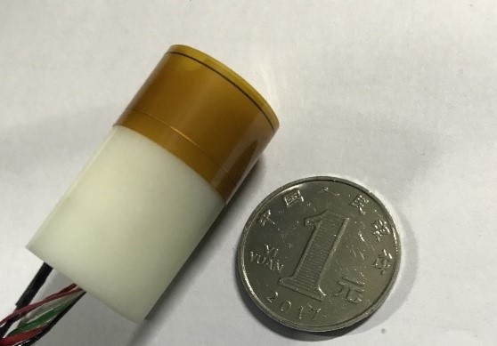
We use atomic magnetometers to get the information of external fields by measuring the responses of atomic spins. Highly sensitive sensors for low field measurement (<100 nT) with low cost and low power consumption are desired. The figure below shows the first version of the USTC sensor, which is based on the SERF mechanism. Its size is 20 mm×20 mm×35 mm, with the cell temperature of 150 oC, heating power less than 1.5 W, laser power less than 2 mW, a closed loop bandwidth larger than 100 Hz, and the magnetic field sensitivity around 25 fT/Hz1/2 @ 10 Hz.
2. Atomic devices assisted by multipass cavities
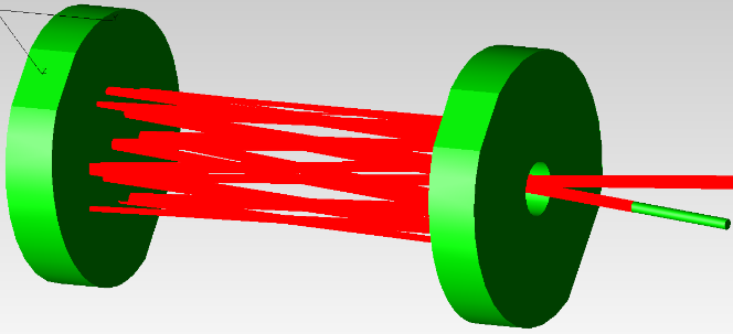
In this topic, we want to improve the sensor sensitivity without increasing its size. In the meantime, we want to standardize the production of the sensor so that we can get rid of the complicated and time-consuming process of optical adjustments. We choose the compact Herriott cavity as the multipass cavity, which has dense optical patterns in a limited space. The figure below shows the simulated optical paths inside one of these cavities.
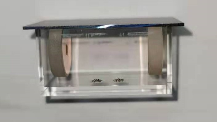
We adapt the anodic bonding technology for the cell production. Under the conditions of high temperature and high voltage, there is a current flowing through the silicon wafer and the cavity mirrors to form a strong chemical bond at the interface of these two materials. The cell based on this technology can be readily used with a pre-designed 3D printing platform as shown in the following picture.
We further set up a vacuum system for anodic bonding, so that we can realize a fully standardized production of the atomic cell inside the vacuum. A sample cell is shown in the following picture.
3. Atomic comagnetometer
An atomic comagnetometer consists of two magnetometers which simultaneously measure the external fields at the same location. Such a setup can largely suppress the drift and noise from the external field. We focus on the hybrid nuclear-spin/electron-spin system, where the nuclear spin atom are hyperpolarized by the electron-spin atoms by spin-exchange collisions. Meanwhile, as shown in the following picture, we can use polarized electron-spin atoms as a sensitive magnetometer to detect the precession signals from the polarized nuclear-spin atoms. Using Xe isotopes-Rb systems, we are working to develop a miniaturized atomic nuclear magnetic resonance gyroscope, and search for anomalous couplings to the nuclear spin.


